
Digital computing and communications are headed toward a future that combines electronics—processing data using electricity—with photonics, which uses light for the same purpose. This integration could enable vastly greater global data flow while also improving energy efficiency.
“In short, merging photonics and electronics in a single package is the 21st-century equivalent of the transistor. Without that breakthrough, future scaling won’t be possible,” says Lionel Kimerling, MIT’s Thomas Lord Professor of Materials Science and Engineering and director of the MIT Microphotonics Center.
FUTUR-IC Aims to Revolutionize Microchip Manufacturing with Resource-Efficient Solutions
That’s where FUTUR-IC comes in—a new MIT-based research team. “Our mission is to develop a microchip industry value chain that uses resources efficiently,” says Anu Agarwal, head of FUTUR-IC and principal research scientist at the Materials Research Laboratory (MRL).
FUTUR-IC researchers, including Anu Agarwal and Lionel Kimerling, have developed a new method for co-packaging photonic and electronic chips that addresses key limitations of existing approaches. A major benefit is that manufacturers can use standard tools and low-cost passive alignment to produce the device more economically.
The patented device was featured on the cover of Advanced Engineering Materials earlier this year. A related paper by DMSE student Drew Weninger won Best Student Paper at last fall’s 57th International Symposium on Microelectronics.
Weninger, Kimerling, Agarwal, Serna (Bridgewater State), and Ranno (MIT) co-authored the paper.
Advancing a More Resource-Efficient Microchip Sector
Kimerling points out that by 2020, more than 50 billion devices—including cell phones and GPS systems—will connect to the cloud, driving demand on large-scale data centers. Meanwhile, the amount of data flowing through these centers is increasing a thousandfold every decade.
This surge in communication consumes energy. “And we have to meet that demand without increasing energy use, since the global economy isn’t growing as fast,” says Kimerling, who is also affiliated with the MRL. To address this, we must either boost energy production or improve the energy efficiency of information technology.

Integrating Photonics and Electronics to Tackle the Microchip Energy Crisis
Merging photonics with the electronics found in modern microchips could help solve energy efficiency issues, since transmitting data with light is far more energy-efficient than using electricity. “Our guiding principle is to rely on electronics for computation and photonics for communication in order to manage the energy crisis,” explains Agarwal.
But this approach presents significant obstacles.
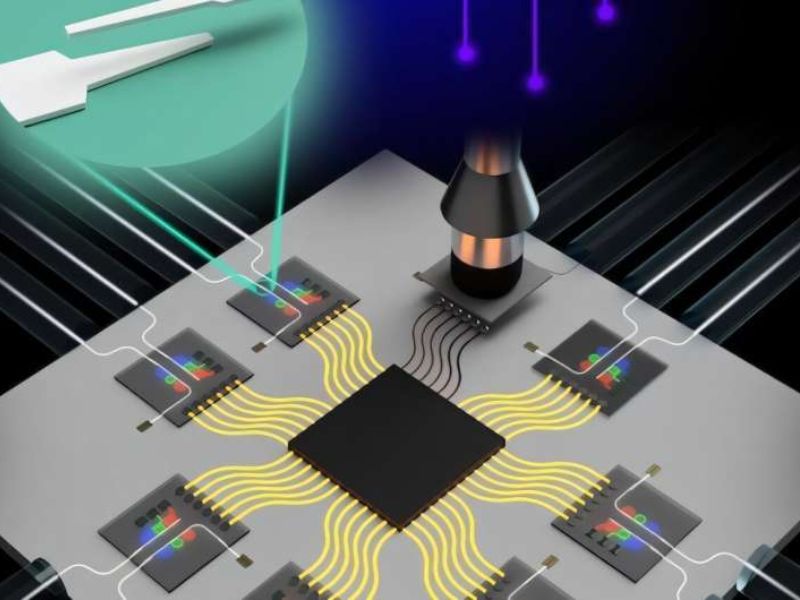
One major challenge is the high cost and complexity of linking electronic and photonic chips within the same unit. Optical fibers have cores that are just ten micrometers wide, while photonic chips have tiny cross-sections—only 0.2 by 0.5 micrometers—requiring extremely precise alignment to prevent light from scattering. Currently, technicians must test each connection individually with a laser to confirm proper light transmission.
“And with the growing demand for higher data capacity, the number of fiber connections is rising rapidly,” Weninger noted. “This active alignment method won’t be sustainable for scaling in the future.”
Greater Flexibility
The newly developed device, known as an evanescent coupler, significantly eases the challenge of aligning fibers within an electronic-photonic system. “Traditional couplers rely on a single coupling point, which demands extremely precise alignment,” explains Agarwal. “Our coupler, however, features a longer interaction region, which greatly relaxes those alignment requirements.” This improvement allows for passive robotic assembly of the integrated circuits, enabling more efficient light transmission without the need for active laser alignment.
Another notable breakthrough, according to Ranno, is that the coupler enables vertical light transmission between the multiple chip layers. This is a major advancement, as guiding light out of the horizontal plane is typically very challenging.
“In electronics, moving electrons between layers is straightforward,” says Weninger. “But light doesn’t naturally bend at sharp angles.” The new design overcomes this limitation, allowing optical signals to travel between stacked chips.
Ranno summarizes: “We’ve created a photonics-electronics integration design that’s space-efficient, dependable, tolerant of alignment variations, and minimizes light loss—essentially, it checks all the boxes for a high-performance interconnect.”
This work was carried out in part through the use of facilities at MIT.nano, and includes contributions from MIT’s Electronic-Photonic Packaging Consortium.
Read the original article on: Tech Xplore
Read more: What Can You Actually Do With Unitree’s $6,000 Humanoid Robot?