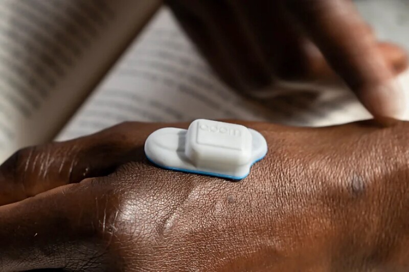

Researchers at Empa, EPFL, and CSEM have created an eco-friendly smart sensing tag that tracks temperature and humidity in real time and can indicate when a temperature limit has been crossed. It could eventually be used to monitor sensitive goods like pharmaceuticals or food. The tag is fully biodegradable.
Every day, vast quantities of sensitive goods—like vaccines, medicines, and perishable foods—travel globally. Maintaining strict temperature and humidity limits is crucial, but equipping each shipment with conventional sensors is costly, unsustainable, and provides limited insight into conditions along the route.
A Four-Year Effort Leads to a Fully Biodegradable Smart Sensor Tag
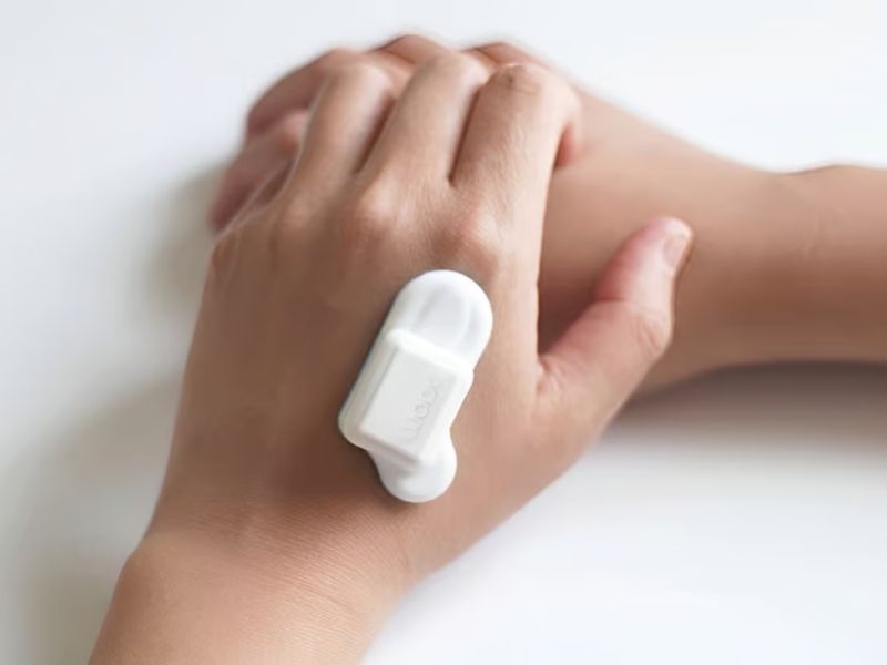
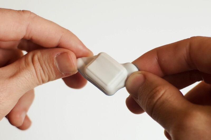
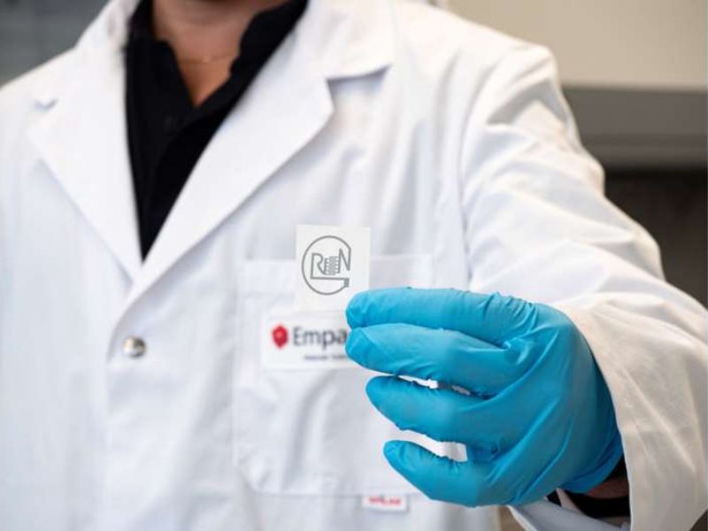
In response to this problem, researchers at Empa, EPFL, and CSEM have spent four years working on the Greenspack project. They have created an innovative sensor tag that tracks temperature and relative humidity and can log when a critical temperature threshold has been surpassed. This tiny, sticker-like device contains no silicon and is fully biodegradable. The team has reported its results in Nature Communications.
The smart tag operates without a battery or transmitter. Instead, it functions much like an RFID device. It uses printed conductive pathways that create electrical circuits made up of resistive and capacitive components. When exposed to an electromagnetic field, the circuits generate a resonance signal that the reader can detect.

The circuits’ conductivity and capacitance change with temperature or humidity, altering their resonance. This shift reveals the surrounding temperature and moisture levels—eliminating the need for complex sensing electronics.
Smart Tag Records Irreversible Heat Events Above 25 °C
The team also added a built-in “memory”: if temperatures exceed 25 °C, a tiny circuit component melts and breaks permanently. At the next scan, the tag reveals that the shipment was exposed to excessive heat. “For vaccines, this could make the batch unusable or expire,” says Gustav Nyström, head of Empa’s Cellulose and Wood Materials lab.
This approach reduces supply chain strain and environmental impact by detecting compromised goods early, allowing rerouting of items with reduced shelf life. “By choosing different materials, we can define various temperature thresholds,” Nyström adds. Tags designed specifically for frozen products are one potential application.
After a shipment arrives, the tag is intended to be composted or recycled with cardboard, since it is entirely biodegradable. For the base material, the Empa team developed a special substrate made from a biopolymer combined with cellulose fibers. Empa and EPFL researchers then printed the conductive sensing structures using a tailored ink that contains the bio-absorbable metal zinc. At the same time, CSEM focused on designing the tag and developing the readout system.
Overcoming the Challenges of Biodegradable Sensor Design
Using biodegradable materials poses its own difficulties—they must remain stable until their job is complete. Moreover, each sensing component had to react only to its specific environmental factor. “We didn’t want the temperature sensor to respond to humidity, or the humidity sensor to react to temperature,” Nyström explains. Working together, the partners succeeded in addressing these challenges.
Two EPFL researchers are now moving toward commercializing the Greenspack results through a start-up called Circelec. Meanwhile, Nyström’s team at Empa plans to advance their research in green electronics and investigate how smart biodegradable labels could be used in agriculture and environmental monitoring.
Read the original article on: Techxplore
Read more: Selfie-Based Age Checks Rise Amid Stricter Online Rules